IBM 2nm chip breakthrough claims more power with less energy
 Getty Images
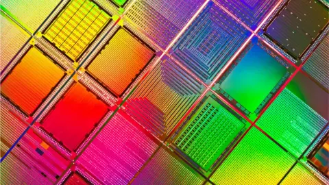
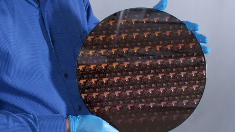
IBM says it has made a significant breakthrough in computer processors by creating a 2nm chip in its test lab.
The process used to make computer chips is measured in nanometres (nm) - with a lower number usually signifying a leap forward.
IBM claims its test chip can improve performance by 45% over current 7nm commercially available products.
It is also more energy efficient - using 75% less energy to match current performance, IBM said.
It claims the tech could "quadruple" mobile phone battery life, and phones might only need to be charged every four days.
The computer chip industry used to use nanometres - one billionth of a metre - to measure the physical size of transistors. Today, a lower "nm" number is widely seen as a marketing term to describe new generations of the technology, leading to better performance and lower power.
 IBM
IBMIBM says its 2nm process can cram 50 billion transistors into "a chip the size of a fingernail" - up from 30 billion when it announced its 5nm breakthrough in 2017.
The end result should be another performance bump for computers in the coming years.
'A breakthrough'
Current high-end desktop chips based on the 7nm process, such as AMD's Ryzen processors, did not become widely available until 2019 - four years after IBM announced it had cracked the 7nm process.
But mainstream commercial chip-makers such as Intel and TSMC - which makes AMD processors - have already said they plan to build ultra-low nm chip plants in the next several years.
"This can be considered as a breakthrough," said Peter Rudden, research director at market intelligence firm IDC.
 IBM
IBM"We have seen semiconductor manufacturers moving from 14nm to 10nm to 7nm, with 7nm being a real challenge for some," he explained.
He said IBM's new process could be used for AI uses that today need a second piece of tech - such as a powerful graphics card- to handle some tasks. The increased power efficiency could be useful in personal devices, while increased performance would benefit huge datacentres, he added.
"This also sends a message to the IT industry that IBM continues to be a hardware research powerhouse."
Chip wars
IBM said the test chip for its 2nm process was built at its Albany research lab in the United States.
The news comes amid an international shortage of computer chips and a bid to shake up chip manufacturing to rely less on major foundries in China and Taiwan.
Car manufacturers have been forced to suspend production due to the lack of computer parts; smartphone makers have warned product releases could be affected; and high-end computer components such as graphics cards are difficult to find and selling for high prices.
On Thursday, Nintendo joined the chorus of concerned companies, saying the chip shortage was affecting production of its hugely popular Nintendo Switch console.
The worldwide shortage led US President Joe Biden to convene a special industry summit on the shortage. In the UK, the government has intervened in the acquisition of chip designer Arm by tech giant Nvidia.
And Intel's chief executive has announced a $20bn (£14.6bn) investment in two new plants in the US, telling the BBC that having 80% of the world chip supply in Asia is not a good idea.
